Parts Inventory | ||
| Designation | Value | Marking |
|---|---|---|
| Resistors | ||
| R1, R6, R11, R16, R29 (optional) | 1kΩ | Brown-Black-Red |
| R2, R7, R9, R14, R17, R20, R24 | 47kΩ | Yellow-Violet-Orange |
| R3, R27, R28 | 270Ω | Red-Violet-Brown |
| R4, R8, R10, R15 | 10kΩ | Brown-Black-Orange |
| R5, R18 | 100kΩ | Brown-Black-Yellow |
| R12 | 1MΩ | Brown-Black-Green |
| R13 | 33kΩ | Orange-Orange-Orange |
| R19 | 4.7kΩ | Yellow-Violet-Red |
| R21 | 3.3kΩ | Orange-Orange-Red |
| R22 | 470kΩ | Yellow-Violet-Yellow |
| R23, R25, R26 | 10Ω | Brown-Black-Black |
| W1, W2, W3 | 10kΩ Potentiometer | 10K |
| Capacitors | ||
| C1, C16, C21, C22, C23, C24, C25, C26, C27, C28 | .1uF | 104 |
| C2, C5, C6, C13, C17 | 1000pF | 102 |
| C3, C4 | 2pF | 2 |
| C7, C8, C9 | 47pF | 47 |
| C10, C14 | 27pF | 27 |
| C11 | 10pF | 10 |
| C12, C15, C18, C19, C20 | .01uF | 103 |
| C29 | .47uF | 474 |
| Electrolytic capacitors | ||
| CP1, CP2, CP5, CP8 | 100uF | |
| CP3, CP4, CP6, CP7, CP9, CP10, CP11 | 10uF | |
| Transistors | ||
| Q1, Q2 | 3355 NPN (TO-92 pkg) | 2SC3355 |
| ICs | ||
| U1 | 8V Voltage Regulator | 78L08 |
| U2 | NE602 Mixer | NE602/SA602 or NE612/SA612 |
| U3 | MC1350 IF amplifier | MC1350 |
| U4, U5 | LM358 dual op-amp | LM358 |
| U6 | LM386 audio amplifer | LM386 |
| Diodes | ||
| D1 | BB910 varicap (TO-92 pkg) | BB910 |
| D2 | Germanium signal diode | |
| D3 | 1N4001 | |
| D4 | 1N4148 | 4148ST |
| Z1, Z2 | Zener Diode | |
| Misc | ||
| Y1 | 10.7MHz Ceramic Resonator | L10.7 |
| L1 | Variable Inductor | |
| J1 | BNC | |
| J2 | Power (center positive) | |
| J3 | 3.5mm audio jack | |
Assembly steps | ||
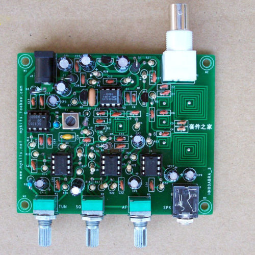
| 1. | To begin, sort the parts into similar groups and place them on a piece of white paper. Use a multimeter or part identifier to confirm part values. Write the values for each component (or group of components) on the paper. This makes placing the resistors in the correct holes much easier. |  |
| 2. | Identify, place and install the ceramic capacitors and C29 in their respective locations. (Do not install the electrolytic capacitors yet). |  |
| 3. | Install the L1 and the IC sockets for U1-U4. (Do not install the ICs yet.) Be sure to orient the sockets as shown on the PCB. |  |
| 4. | Install the 10.7MHz ceramic resonator (Y1). Pin one is the hole with the square solder pad. |  |
| 5. | Identify, place and install the fixed-value resistors (Do not install the potentiometers (W1-W3) yet). |  |
| 6. | Identify, place and install the diodes (D1-D4, Z1 and Z2). Be sure to orient the components as shown on the PCB. (Note: the line on the diode casing corresponds to the line on the diode symbol on the PCB - this is the cathode. For this kit, the cathode lead will point upward and bend over to the neighboring through-hole.) For D1, orient as shown on the PCB. |  |
| 7. | Install the 3.5mm audio jack (J3) |  |
| 8. | Identify, place and install the transistors and voltage regulator (Q1, Q2 & U1). You may need to bend the leads of the transistors outward ever so slightly to align with the holes in the PCB. The body of the transistors will rest about 1/8" above the PCB. Do not force it all the way down to the board or you could damage the component. |  |
| 9. | Install the transformer (T1) and the electrolytic capacitors (CP1-CP11). Electrolytic capcitors have an anode and cathode. The longer lead is the anode (+) and is noted on the board. The cathode (-) is marked on the body of the capacitor and the proper orientation is marked on the PCB. |  |
| 10. | Install the potientiometers (W1-W3) on the front of the board and J1 and J2 on the back of the board. Be sure the body of the component is perpendicular to the PCB. |  |
| 11. | Install the ICs U2-U6 into their corresponding sockets being sure to align each IC correctly. (Pin 1 is usually denoted with a dot or impression on the package or simply align the notch on the end of the package with that on the socket.) | |
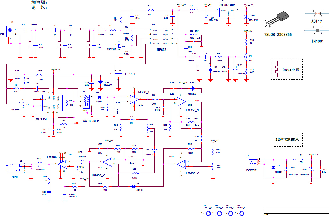
Schematic
Below is the schematic diagram of the receiver, taken from the manufacturer's manual.